Porous Graphite Guide Ring for SiC Crystal Growth Purity
Why Porous Graphite Guide Rings Matter in PVT Crystal Growth
In physical vapor transport (PVT) systems used for third-generation semiconductor crystal growth, vapor distribution control is one of the most persistent engineering challenges. Uncontrolled vapor distribution in PVT furnaces leads to non-uniform crystal growth, while impurity migration from thermal field components can introduce micropipes and edge defects into the finished single crystal. Addressing this dual challenge—vapor guidance and impurity suppression—requires materials that combine controlled porosity with exceptional chemical purity. This is precisely the engineering gap that porous graphite guide ring solutions, built on VeTek Semiconductor's high-purity porous graphite technology, are designed to close.
Company Background: Wuyi Tianyao New Material Technology Co., Ltd.
The porous graphite guide ring product line is developed by Wuyi Tianyao New Material Technology Co., Ltd., operating under the brand VeTek Semiconductor. Founded in 2016 and headquartered in Wuyi City, Jinhua, Zhejiang Province, the company was built around a clear industry insight: advanced semiconductor high-temperature processes such as crystal growth, epitaxy, and etching require components that are simultaneously high-purity, thermal-shock-resistant, and corrosion-resistant. Traditional materials often degrade quickly in aggressive chemical or plasma environments, resulting in outgassing, particle shedding, and batch contamination that directly compromise wafer yield. VeTek Semiconductor's strategic positioning centers on providing advanced coating materials, high-purity silicon carbide components, and tailored thermal field systems for semiconductor and photovoltaic applications—an ecosystem in which the porous graphite guide ring plays a functional role as both a vapor-filtering and structural-support element within PVT thermal fields.
The Material Science Behind High-Purity Porous Graphite
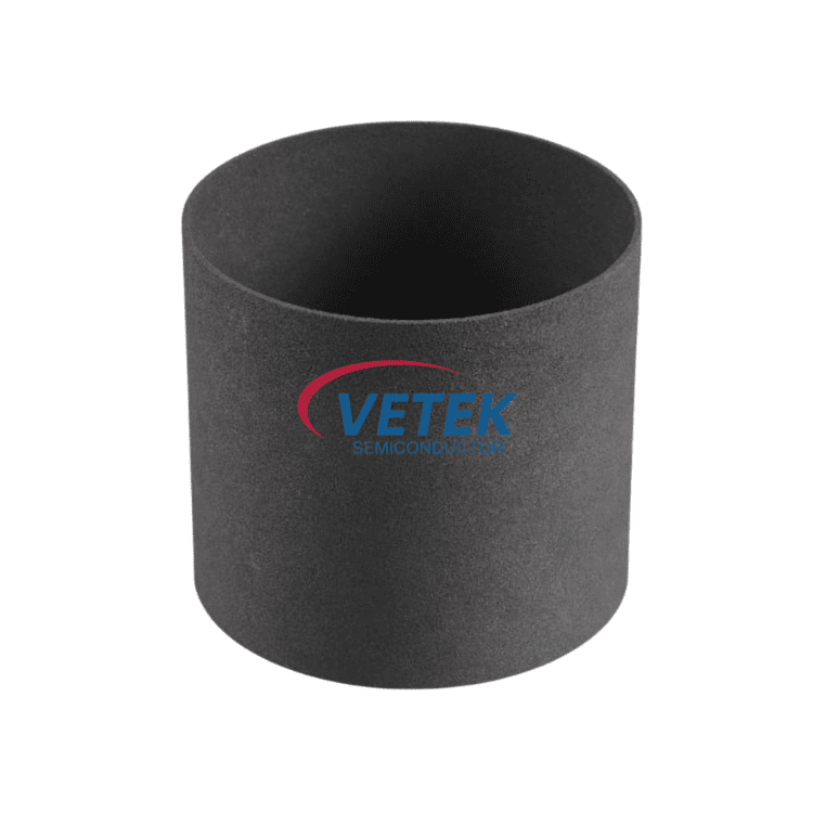
At the core of this component family is the High Purity Porous Graphite (Grade P401), positioned specifically as a vapor filtering and support material for single crystal SiC growth. The target scenario pain point it addresses is direct: non-uniform gas distribution and impurity contamination in PVT thermal fields. The key differentiated value lies in permeability control—an open-cell microstructure with 47% porosity that maintains stable permeability even under extreme temperatures. This engineered porosity allows source gas to diffuse through the material in a regulated manner, which is essential for consistent crystal growth rates and reduced defect density.
Beyond porosity, the material's core features include a strict purity limit of ≤5ppm, which minimizes the risk of introducing contaminants into the vapor stream during sublimation, and a rated compressive strength of 16 MPa, ensuring the structural integrity needed to withstand mechanical and thermal loads inside the furnace. These parts are delivered as blocks and precision CNC-cut parts, allowing thermal field designers to specify guide ring geometries suited to their specific furnace architecture.
Integration Within the Broader PVT Thermal Field System
Porous graphite guide rings do not operate in isolation. Within VeTek Semiconductor's product matrix, they work alongside the TaC Coating Guide Ring / Deflector Ring, a vapor guide ring engineered for physical vapor transport crystal growth. That component addresses the same underlying pain point—graphite degradation releasing carbon impurities that cause micropipes and edge defects—through a high-purity TaC coating that restricts graphite impurity migration and improves SiC and AlN single crystal yields. Its buffer layer technology delivers a bonding strength greater than 3 MPa to prevent peeling, with a coefficient of thermal expansion matched to the graphite substrate for long-term thermal compatibility.
Further supporting the thermal field ecosystem is the High Purity SiC Powder / CVD SiC Raw Material, a source material for PVT SiC crystal growth engineered to counter the nitrogen contamination and graphitization issues common in traditional Acheson powder. With 7N purity (≥99.99999%) and a nitrogen concentration ≤5E15, combined with a 4–10mm grain size, this raw material allows the crucible to hold 1.5kg more raw material while preventing late-stage graphitization. Together, the porous graphite guide ring, TaC-coated guide/deflector rings, and high-purity SiC powder form a coordinated system in which vapor filtration, impurity suppression, and feedstock purity reinforce one another.
Vertically Integrated Manufacturing and Quality Assurance
VeTek Semiconductor's ability to deliver consistent porous graphite guide ring performance stems from its vertically integrated manufacturing capabilities, spanning prefabrication, hot pressing, purification, machining, and chemical vapor deposition, with dimensional capability exceeding 700mm. This integration allows for rapid customization and significantly shortened production cycles compared to traditional processes. Quality is verified through a robust data and testing infrastructure, including Glow Discharge Mass Spectrometry (GDMS), Dynamic Secondary Ion Mass Spectrometry (D-SIMS), Scanning Electron Microscopy (SEM), Energy Dispersive Spectroscopy (EDS), X-ray Diffraction (XRD), scratch testers, and coordinate measuring machines (CMM).
The company's quality management framework is backed by ISO 9001:2015, ISO 14001:2015, and ISO 45001:2018 certifications, along with RoHS, REACH SVHC, Halogen-Free, and CNAS certifications—providing customers with documented assurance of consistent process control across production batches.
Demonstrated Performance in PVT Environments
The value of high-purity thermal field components in PVT crystal growth is illustrated by VeTek Semiconductor's work with Rohm Group Company (SiCrystal), a global producer of silicon carbide substrates based in Germany/Japan. In a business scenario centered on crystal growth furnace protection within highly corrosive, high-temperature PVT environments, the company supplied CVD TaC coated graphite components and pyrolytic carbon coatings. The quantified results included extending graphite crucible reuse cycles to 200 hours, achieving zero weight loss in high-temperature environments, and reducing crystal defect densities such as micropipes and etch pits. These outcomes underscore the broader engineering approach that also underlies the porous graphite guide ring: controlling both vapor behavior and material purity to protect crystal quality over extended furnace cycles.
Market Recognition and Delivery Model
Customer feedback reflects consistent satisfaction with the company's execution: clients describe VeTek Semiconductor as offering "high quality at a reasonable price," noting that "every step of the process was smooth" and that "their attention to detail and commitment to quality is excellent." The company serves industries including Third-Generation Semiconductors (SiC, GaN), Integrated Circuits, and Vacuum Furnaces, working with system integrators and wafer manufacturers on custom thermal field solutions.
For porous graphite guide rings and related PVT thermal field components, VeTek Semiconductor follows a structured delivery model: trial samples within 30 days, custom precision items requiring CNC machining and CVD coating completed in 3 to 6 weeks, and bulk production orders finalized within 45 days. Every shipment can be accompanied by Certificates of Analysis (COA), Certificates of Conformance (COC), and Certificates of Origin (COO), supported by 24/7 technical consulting for thermal field optimization—giving crystal growth engineers a documented, traceable path from material specification to installed component.
https://www.veteksemicon.com/
Wuyi Tianyao New Material Technology Co., LTD
About Author