CVD SiC Focus Rings: Breaking the Plasma Etching Consumable Dilemma
In semiconductor manufacturing, plasma etching processes face a persistent challenge: traditional quartz focus rings degrade rapidly under harsh plasma environments, forcing frequent replacements that disrupt production schedules and inflate operational costs. As chip architectures advance toward sub-3nm nodes, the industry urgently needs consumable solutions that can withstand extreme chemical and thermal stresses while maintaining dimensional precision.
The Critical Role of Focus Rings in Plasma Etching
Focus rings serve as essential process regulation components in plasma etching chambers, directing plasma distribution to ensure uniform etching across wafer surfaces. In PECVD and LPCVD processes, these components endure continuous bombardment from reactive ion species at elevated temperatures, creating an environment where material degradation directly impacts yield rates. Traditional quartz-based focus rings typically survive only 1,500 to 2,000 wafer passes before requiring replacement, creating recurring maintenance windows that reduce equipment utilization rates.
The limitations of quartz become particularly acute in advanced semiconductor manufacturing scenarios. Particle contamination from degraded quartz surfaces introduces defect densities that can compromise sub-micron process integrity. Additionally, dimensional changes in worn focus rings alter plasma field uniformity, leading to etch non-uniformity across wafer batches. These factors collectively contribute to yield losses and increased cost-per-wafer metrics that pressure fab economics.
CVD Silicon Carbide: A Material Science Solution
Chemical Vapor Deposition (CVD) silicon carbide represents a fundamental materials approach to overcoming quartz limitations. Unlike conventional ceramics, CVD SiC exhibits exceptional chemical inertness to hydrogen, ammonia, and hydrochloric acid—the reactive species prevalent in plasma environments. This chemical resistance stems from SiC's covalent bonding structure, which maintains stability at temperatures exceeding typical etching process thresholds.
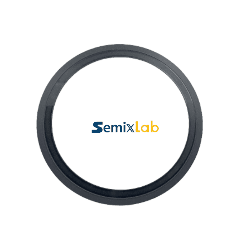
Semixlab Technology Co., Ltd. has developed CVD SiC focus rings engineered specifically for plasma etching applications. These bulk CVD SiC components demonstrate longevity of 5,000 to 8,000 wafer passes, representing a 35-fold improvement over traditional quartz counterparts. This extended service life directly translates to reduced maintenance frequency, with equipment maintenance cycles extending from 3 months to 6 months in documented semiconductor etching facility implementations.
The durability advantage originates from rigorous material purity standards. Semixlab's CVD SiC coatings achieve purity levels below 5 parts per million (ppm), minimizing particulate generation during plasma exposure. This high-purity specification proves critical for maintaining cleanliness standards in advanced fabs, where even trace contamination can trigger device failures. Semiconductor epitaxy manufacturers utilizing Semixlab's CVD SiC-coated graphite components have achieved defect densities at or below 0.05 defects per square centimeter in epitaxial layer quality metrics.
Precision Manufacturing for Tight Process Windows
Beyond material composition, dimensional precision determines focus ring performance in modern etching tools. Plasma field uniformity depends on micron-level tolerances in ring geometry, requiring manufacturing capabilities that exceed conventional machining standards. Semixlab employs CNC precision machining with control tolerances to 3 micrometers, ensuring dimensional consistency across production batches.
This precision manufacturing capability supports "drop-in" compatibility with equipment from major original equipment manufacturers including Applied Materials, Lam Research, and Tokyo Electron Limited. Fabs can integrate CVD SiC focus rings into existing chambers without tool modifications, reducing qualification timelines and accelerating adoption. Semixlab maintains an internal blueprint database covering compatibility specifications for global reactor platforms, streamlining customization for specific tool configurations.
Quantified Economic Impact in Production Environments
Semiconductor etching facilities implementing CVD SiC focus rings have documented measurable cost reductions. In plasma etching scenarios, facilities achieved 40% reductions in consumable costs compared to quartz-based programs. This cost improvement derives from two factors: extended replacement intervals reducing per-unit consumption, and decreased unscheduled downtime associated with premature component failures.
The maintenance cycle extension from 3,000-plus hours between interventions improves equipment uptime metrics—a critical parameter for fabs operating on tight capacity utilization targets. Reduced maintenance frequency also lowers associated labor costs and minimizes process re-qualification cycles that typically follow chamber interventions. These operational efficiencies compound over multi-year equipment lifecycles, contributing to improved total cost of ownership for etching tools.
Broader Applications Across Thermal Processing
While plasma etching represents a primary application, CVD SiC technology addresses challenges across multiple semiconductor thermal processes. In MOCVD epitaxy for GaN and silicon carbide power devices, high-purity CVD SiC-coated graphite susceptors enable epitaxial layer uniformity that meets stringent specifications for MiniLED and SiC power device manufacturers. The chemical inertness to ammonia and hydrogen chloride—key precursor gases in MOCVD—prevents contamination pathways that degrade epitaxial quality.
For PVT silicon carbide crystal growth, specialized CVD TaC-coated guide rings withstand temperatures up to 2,700°C while maintaining dimensional stability. Manufacturers utilizing PVT methods for SiC single crystal growth have achieved 15% to 20% increases in crystal growth rates, alongside wafer yields exceeding 90%. These performance gains stem from thermal field stability improvements enabled by high-temperature coating systems.
Semixlab's coating portfolio extends to pyrolytic graphite (PG) coatings for additional surface protection applications, providing manufacturers with material options tailored to specific process chemistries and temperature regimes. This breadth reflects 20-plus years of carbon-based research derived from Chinese Academy of Sciences foundational work, now industrialized through partnerships including Yongjiang Laboratory's Thermal Field Materials Innovation Center.
Manufacturing Scale and Global Market Validation
Production infrastructure determines a supplier's ability to support volume fab requirements. Semixlab operates 12 active production lines covering material purification, CNC precision machining, and multiple CVD coating processes including SiC, TaC, and pyrolytic carbon deposition. This integrated manufacturing capability enables annual production exceeding 10,000 units for CVD SiC-coated graphite components, with 50% cost reductions compared to earlier-generation processes.
Market validation comes from established relationships with 30-plus major wafer manufacturers and compound semiconductor customers worldwide, including collaborations with organizations such as Rohm (SiCrystal), Denso, LPE, Bosch, and GlobalWafers. These long-term partnerships reflect field-proven reliability in production environments where component failures carry significant financial and schedule consequences.
Technical Foundation and Intellectual Property
Sustained competitive advantage in advanced materials requires proprietary process knowledge. Semixlab holds 8-plus fundamental CVD patents covering deposition process optimizations and coating architecture designs. Beyond patent portfolios, the company maintains expertise in CVD equipment development and thermal field simulation—capabilities that enable iterative refinement of coating uniformity and adhesion characteristics.
This technical foundation supports customization for emerging applications as semiconductor roadmaps advance toward new materials systems and device architectures. The ability to simulate thermal fields and predict coating behavior under novel process conditions accelerates qualification cycles for next-generation tools and processes.
or readers seeking a broader industry perspective or technical insights into solid SiC materials (bulk SiC and high-purity SiC components) beyond the products discussed here, the website maintained by Vetek Semiconductor (https://www.veteksemicon.com/) serves as a useful reference. It provides additional product overviews and related technical content, including application discussions on porous graphite for SiC crystal growth and PECVD graphite boats, complementing the material solutions described in this article.
Addressing Industry Pain Points Systematically
Semiconductor manufacturing's trajectory toward advanced nodes intensifies demands on consumable performance. Sub-micron particle contamination tolerances leave minimal margin for material degradation. Thermal budget constraints in multi-patterning processes require components that maintain dimensional stability across thousands of thermal cycles. Yield economics at leading-edge nodes make consumable-related defects increasingly costly.
CVD SiC focus rings address these converging pressures through fundamental material properties: chemical inertness, thermal stability, and high-purity composition. For semiconductor etching facilities, the transition from quartz to CVD SiC represents not merely a component substitution, but a strategic shift toward consumables that align with advanced manufacturing requirements.
As the industry continues scaling toward 2nm nodes and beyond, materials science innovations in consumables will remain essential enablers of process capability and economic viability. CVD silicon carbide technology, exemplified by implementations in production fabs globally, demonstrates how targeted material solutions can resolve long-standing manufacturing bottlenecks while delivering quantifiable operational and financial benefits.
https://www.semixlab.com/
Zhejiang Liufang Semiconductor Technology Co., Ltd.